


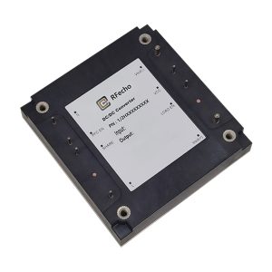
OHI-24-C-028-007-P 18-36 V Input, 28 V/7.5 A Output Half-Brick

High operating efficiency up to 92% with minimal power derating at full rated load.
Wide 18-36 V input voltage range featuring fixed-frequency switching for predictable EMI.
Industry-standard half-brick footprint and pin-out with optional flanged baseplate for mounting flexibility.
Comprehensive protection suite including input UVLO/OV, output current limit, short circuit, and thermal shutdown.
Advanced control capabilities featuring remote sense, wide output trim range, and On/Off functionality.
Full compliance with international UL/CSA/EN 60950-1 safety standards and RoHS directives.
Reliable performance with no minimum load requirement and active back-drive current limiting.
- Description
- Datasheet
- Reviews (0)
Description
The OHI-24-C-028-007-P half-brick converter series is composed of next-generation, board-mountable, isolated, fixed switching frequency dc-dc converters that use synchronous rectification to achieve extremely high power conversion efficiency. Each module is supplied completely encased to provide protection from the harsh environments seen in many industrial and transportation applications.
OHI-24-C-028-007-P | |
| OHI-24-C-028-007-P 18-36 V Input, 28 V/7.5 A Output Half-Brick | |
Property | Value |
| Maximum Input Current (Max.) | 17.0 A |
| Maximum Input Current (Notes & Conditions) | Vin min; trim up; in current limit |
| No-Load Input Current (enabled) (Typ.) | 140 mA |
| No-Load Input Current (enabled) (Max.) | 180 mA |
| Disabled Input Current (Typ.) | 1.5 mA |
| Disabled Input Current (Max.) | 3 mA |
| Response to Input Transient (Typ.) | 1.2 V |
| Response to Input Transient (Notes & Conditions) | See Figure 6 |
| Input Terminal Ripple Current (Typ.) | 250 mA |
| Input Terminal Ripple Current (Notes & Conditions) | RMS |
| Recommended Input Fuse (Max.) | 20 A |
| Recommended Input Fuse (Notes & Conditions) | Fast acting fuse recommended |
| Output Voltage Set Point (Min.) | 27.72 V |
| Output Voltage Set Point (Typ.) | 28.00 V |
| Output Voltage Set Point (Max.) | 28.28 V |
| Over Line (Typ.) | +/-0.1 % |
| Over Line (Max.) | +/-0.3 % |
| Over Load (Typ.) | +/-0.1 % |
| Over Load (Max.) | +/-0.3 % |
| Over Temperature (Min.) | -420 mV |
| Over Temperature (Max.) | 420 mV |
| Total Output Voltage Range (Min.) | 27.30 V |
| Total Output Voltage Range (Max.) | 28.70 V |
| Total Output Voltage Range (Notes & Conditions) | Over sample, line, load, temperature & life |
| Output Voltage Ripple and Noise (Notes & Conditions) | 20 MHz bandwidth |
| Peak-to-Peak (Typ.) | 150 mV |
| Peak-to-Peak (Max.) | 300 mV |
| Peak-to-Peak (Notes & Conditions) | Full load |
| RMS (Typ.) | 20 mV |
| RMS (Max.) | 40 mV |
| RMS (Notes & Conditions) | Full load |
| Operating Output Current Range (Min.) | 0 A |
| Operating Output Current Range (Max.) | 7.5 A |
| Operating Output Current Range (Notes & Conditions) | Subject to thermal derating |
| Output DC Current Limit Inception (Min.) | 8.3 A |
| Output DC Current Limit Inception (Typ.) | 9.0 A |
| Output DC Current Limit Inception (Max.) | 9.8 A |
| Output DC Current Limit Inception (Notes & Conditions) | Output voltage 10 % Low |
| Output DC Current Limit Shutdown Voltage (Typ.) | 13 V |
| Back-Drive Current Limit while Enabled (Typ.) | 0.16 A |
| Back-Drive Current Limit while Enabled (Notes & Conditions) | Negative current drawn into output pins |
| Back-Drive Current Limit while Disabled (Typ.) | 1 mA |
| Back-Drive Current Limit while Disabled (Notes & Conditions) | Negative current drawn into output pins |
| Maximum Output Capacitance (Max.) | 250 uF |
| Maximum Output Capacitance (Notes & Conditions) | Vout nominal at full load (resistive load) |
| Settling Time (Typ.) | 80 us |
| Settling Time (Notes & Conditions) | To within 1 % Vout nom |
| Output Voltage Trim Range (Min.) | -20 % |
| Output Voltage Trim Range (Max.) | 10 % |
| Output Voltage Trim Range (Notes & Conditions) | Across Pins 8 & 4; Common Figures 3-5 |
| Output Voltage Remote Sense Range (Max.) | 10 % |
| Output Voltage Remote Sense Range (Notes & Conditions) | Across Pins 8 & 4 |
| Output Over-Voltage Protection (Min.) | 32.8 V |
| Output Over-Voltage Protection (Typ.) | 34.2 V |
| Output Over-Voltage Protection (Max.) | 35.6 V |
| Output Over-Voltage Protection (Notes & Conditions) | Over full temp range |
| 100 % Load (Typ.) | 91 % |
| 100 % Load (Notes & Conditions) | See Figure 1 for efficiency curve |
| 50 % Load (Typ.) | 93 % |
| 50 % Load (Notes & Conditions) | See Figure 1 for efficiency curve |
| Operating Input Voltage Range (Min.) | 18 V |
| Operating Input Voltage Range (Typ.) | 24 V |
| Operating Input Voltage Range (Max.) | 36 V |
| Operating Input Voltage Range (Notes & Conditions) | 50 V transient for 1 s |
| Turn-On Voltage Threshold (Min.) | 17.1 V |
| Turn-On Voltage Threshold (Typ.) | 17.5 V |
| Turn-On Voltage Threshold (Max.) | 17.9 V |
| Turn-Off Voltage Threshold (Min.) | 16.0 V |
| Turn-Off Voltage Threshold (Typ.) | 16.5 V |
| Turn-Off Voltage Threshold (Max.) | 16.9 V |
| Lockout Voltage Hysteresis (Typ.) | 1.0 V |
| Input Over-Voltage Shutdown (Min.) | 52 V |
| Input Over-Voltage Shutdown (Typ.) | 55 V |
| Recommended External Input Capacitance (Typ.) | 470 uF |
| Recommended External Input Capacitance (Notes & Conditions) | Typical ESR 0.1-0.2 Ohm |
| Input Filter Component Values (LC) (Typ.) | 1.113.2 uH uF |
| Input Filter Component Values (LC) (Notes & Conditions) | Internal values |
| Non-Operating (Min.) | -1 V |
| Non-Operating (Max.) | 60 V |
| Non-Operating (Notes & Conditions) | Continuous |
| Operating (Max.) | 36 V |
| Operating (Notes & Conditions) | Continuous |
| Operating Transient (Max.) | 50 V |
| Operating Transient (Notes & Conditions) | 1 s transient, square wave |
| Input to Output (Max.) | 2250 Vdc |
| Input to Baseplate (Max.) | 2250 Vdc |
| Output to Baseplate (Max.) | 2250 Vdc |
| Operating Temperature (Min.) | -40 °C |
| Operating Temperature (Max.) | 100 °C |
| Operating Temperature (Notes & Conditions) | Baseplate temperature |
| Storage Temperature (Min.) | -45 °C |
| Storage Temperature (Max.) | 125 °C |
| Voltage at ON/OFF input pin (Min.) | -2 V |
| Voltage at ON/OFF input pin (Max.) | 18 V |
| Turn-On Time (Typ.) | 10 ms |
| Turn-On Time (Notes & Conditions) | Full load, Vout=90 % nom. (from enable) |
| Start-Up Inhibit Time (Min.) | 180 ms |
| Start-Up Inhibit Time (Typ.) | 200 ms |
| Start-Up Inhibit Time (Max.) | 220 ms |
| Start-Up Inhibit Time (Notes & Conditions) | Figure E |
| Output Voltage Overshoot (Typ.) | 0 % |
| Output Voltage Overshoot (Notes & Conditions) | Maximum Output Capacitance |
| Isolation Voltage (dielectric strength) (Notes & Conditions) | See Absolute Maximum Ratings |
| Isolation Resistance (Typ.) | 30 M Ohm |
| Isolation Capacitance (input to output) (Typ.) | 1000 pF |
| Isolation Capacitance (input to output) (Notes & Conditions) | See Note 1 |
| Semiconductor Junction Temperature (Max.) | 125 °C |
| Semiconductor Junction Temperature (Notes & Conditions) | Package rated to 150 °C |
| PCB Temperature (Max.) | 125 °C |
| PCB Temperature (Notes & Conditions) | UL rated max operating temp 130 °C |
| Transformer Temperature (Max.) | 125 °C |
| Maximum Baseplate Temperature, Tb (Max.) | 100 °C |
| Switching Frequency (Min.) | 255 kHz |
| Switching Frequency (Typ.) | 275 kHz |
| Switching Frequency (Max.) | 295 kHz |
| Switching Frequency (Notes & Conditions) | Isolation stage switching freq. is half this |
| Off-State Voltage (Min.) | 2.4 V |
| Off-State Voltage (Max.) | 18 V |
| On-State Voltage (Min.) | -2 V |
| On-State Voltage (Max.) | 0.8 V |
| ON/OFF Control (Notes & Conditions) | Application notes Figures A & B |
| Pull-Up Voltage (Typ.) | 5 V |
| Pull-Up Resistance (Typ.) | 50 k Ohm |
| Over-Temperature Shutdown OTP Trip Point (Typ.) | 125 °C |
| Over-Temperature Shutdown OTP Trip Point (Notes & Conditions) | Average PCB Temperature |
| Over-Temperature Shutdown Restart Hysteresis (Typ.) | 10 °C |
| Calculated MTBF (Telcordia) TR-NWT-000332 (Typ.) | 1.44 10^6 Hrs. |
| Calculated MTBF (Telcordia) TR-NWT-000332 (Notes & Conditions) | Tb = 70 °C |
| Calculated MTBF (MIL-217) MIL-HDBK-217F (Typ.) | 1.20 10^6 Hrs. |
| Calculated MTBF (MIL-217) MIL-HDBK-217F (Notes & Conditions) | Tb = 70 °C |
| Field Demonstrated MTBF (Units) | 10^6 Hrs. |
| Field Demonstrated MTBF (Notes & Conditions) | See our website for details |
| Step Change in Output Current (0.1 A/ us) (Typ.) | 1600 mV |
| Step Change in Output Current (0.1 A/ us) (Notes & Conditions) | 50 % to 75 % to 50 % Iout max |
Features | |
| High operating efficiency up to 92% with minimal power derating at full rated load. | |
| Wide 18-36 V input voltage range featuring fixed-frequency switching for predictable EMI. | |
| Industry-standard half-brick footprint and pin-out with optional flanged baseplate for mounting flexibility. | |
| Comprehensive protection suite including input UVLO/OV, output current limit, short circuit, and thermal shutdown. | |
| Advanced control capabilities featuring remote sense, wide output trim range, and On/Off functionality. | |
| Full compliance with international UL/CSA/EN 60950-1 safety standards and RoHS directives. | |
| Reliable performance with no minimum load requirement and active back-drive current limiting. | |
Applications | |
| Industrial and Transportation applications | |
Reviews
There are no reviews yet.