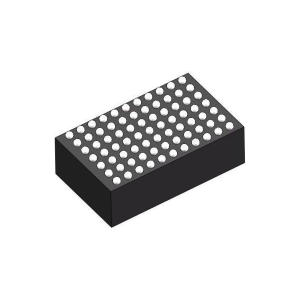
QWB Series — Four-Channel Non-Isolated DC/DC Power Modules

Four independent adjustable outputs in a surface-mount BGA package. Channels may be paralleled using the application circuit shown in the datasheet.
Internal solder-paste melting point
- Part number
- QWB4644M
- Input voltage
- 4–14 Vdc
- Output voltage, selection table
- 0.5–5.5 Vdc¹
- Output current, min. / max.
- 0 / 4 A per channel²
- Efficiency, typ.
- 81 / 75%³
- Ripple, typ.
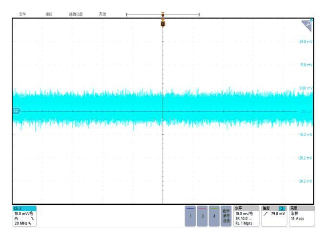
- 30 mVpp
- Operating case temperature
- −55°C to +125°C
- Solder melting point, internal / external
- 238°C / 217°C
¹ Selection table: 0.5–5.5 V; electrical characteristics/application guide: 0.6–5.5 V. Source discrepancy requires confirmation.
² High-temperature maximum: 2 A per channel.
³ Typical efficiency: 81% at high temperature; 75% at room/low temperature, VIN = 5 V / 12 V, VOUT = 1.5 V.
Request a Quote
- Description
- Technical Data
- Datasheet
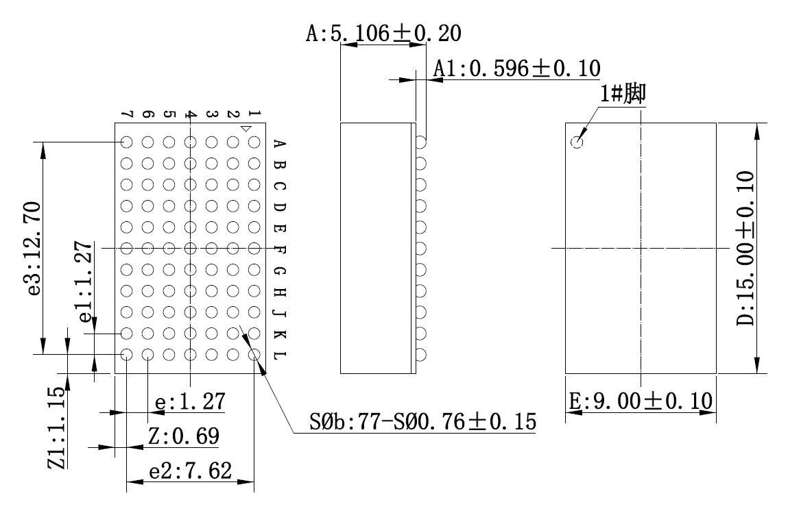
- OUTLINE
QWB4644M — Four-Channel DC/DC Module
The QWB4644M provides four fully independent, non-isolated DC/DC channels. Each channel supports up to 4 A at room/low temperature, with a 2 A rating at high temperature. The output is set by external feedback resistors. Internal solder paste: 238°C; external solder balls: 217°C.
- Input undervoltage, output overcurrent, short-circuit and thermal protection.
- Independent RUN controls, output tracking / soft start and PGOOD indication.
- Four-channel parallel operation is shown as a single 16 A application in the datasheet; applicable temperature limits and current derating still apply.
- Only the two listed M-grade solder configurations are included in this draft.
Application circuits
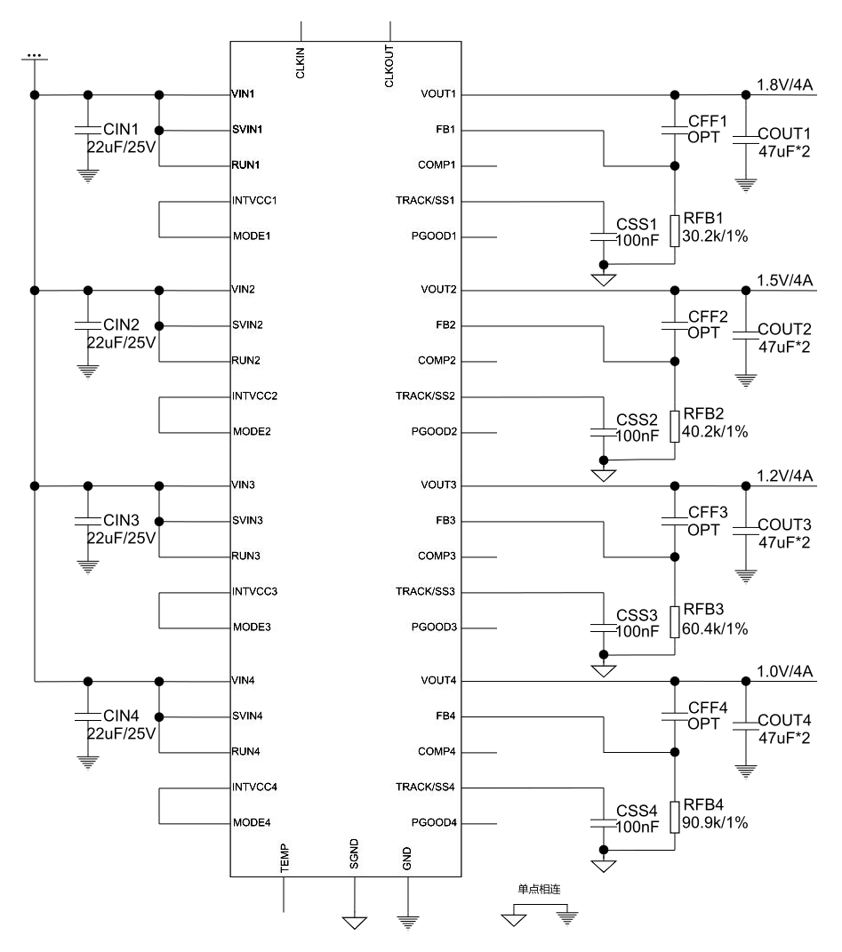
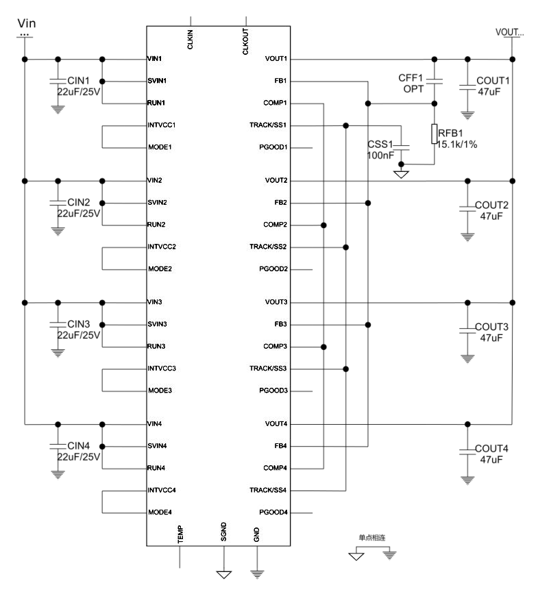
Circuits are retained from the source manual. Single-point connections are identified in the diagrams. Leave unspecified connections open. See the datasheet for pin assignments and application conditions.
Technical Data — QWB4644M
Electrical characteristics; source temperature categories are retained. CIN1–CIN4 = 20 µF and COUT1–COUT4 = 100 µF, as specified in the electrical table notes.
| Characteristic | Test temperature | Min. | Typ. | Max. | Unit | Conditions |
|---|---|---|---|---|---|---|
| Input voltage range | Room / High / Low | 4 | 5 | 14 | V | VIN1–VIN4 |
| Output voltage range | Room / High / Low | 0.6 | — | 5.5 | V | VOUT1–VOUT4; externally adjustable |
| Output current | Room / Low | 0 | — | 4 | A | Per channel |
| Output current | High | 0 | — | 2 | A | Per channel; high-temperature derating |
| Line regulation | Room / High / Low | −1.5 | — | +1.5 | %VO | VIN = 5–12 V; IOUT = 0 A |
| Load regulation | Room / Low | −2 | — | +2 | %VO | VIN = 5 V / 12 V; IOUT = 4 A |
| Load regulation | High | −2 | — | +2 | %VO | VIN = 5 V / 12 V; IOUT = 2 A |
| Output ripple | Room / Low | — | 30 | 50 | mVpp | 20 MHz bandwidth |
| Output ripple | High | — | 30 | 50 | mVpp | 20 MHz bandwidth |
| Efficiency | Room / Low | 68 | 75 | — | % | VIN = 5 V / 12 V; VOUT = 1.5 V |
| Efficiency | High | 77 | 81 | — | % | VIN = 5 V / 12 V; VOUT = 1.5 V |
| Output overcurrent protection | Room | 110 | — | — | %IO | Constant-power mode; automatic recovery after fault removal |
| Output short-circuit protection | Room | — | — | — | — | Constant-power mode; automatic recovery after fault removal |
| RUN function (VOUT1–VOUT4) | Room | — | — | 0.3 | V | VIN = 12 V; IOUT = 0 A; RUN1–RUN4 grounded |
| RUN function (VOUT1–VOUT4) | Room | 1.46 | 1.50 | 1.54 | V | VIN = 12 V; IOUT = 0 A; RUN1–RUN4 connected to 12 V logic |
| PGOOD function (VPGOOD1–VPGOOD4) | Room | 3.10 | 3.50 | 3.60 | V | VIN = 12 V; IOUT = 0 A; 100 kΩ between PGOOD and INTVCC; VOUT within ±10% of nominal |
| Weight | — | 1.5 | 2.0 | 2.5 | g |
Spring-contact fixture resistance may affect measurements; the source recommends PCB-based calibration. See the complete datasheet for terminal definitions, PCB layout, soldering and handling instructions.
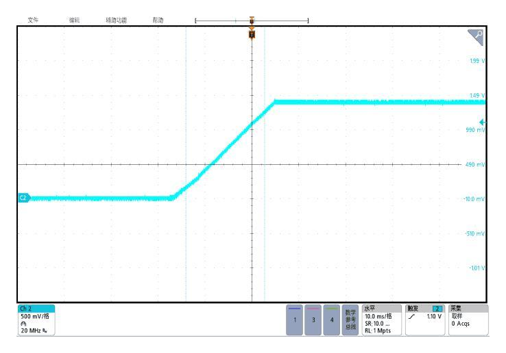
Typical performance curves
Source curves apply to QWB4644M at room temperature.
OUTLINE
Dimensions in mm. Unspecified dimensional tolerance: ±0.25 mm. Shared package for QWB4644M and QWB4644MA.
Recommended PCB land pattern
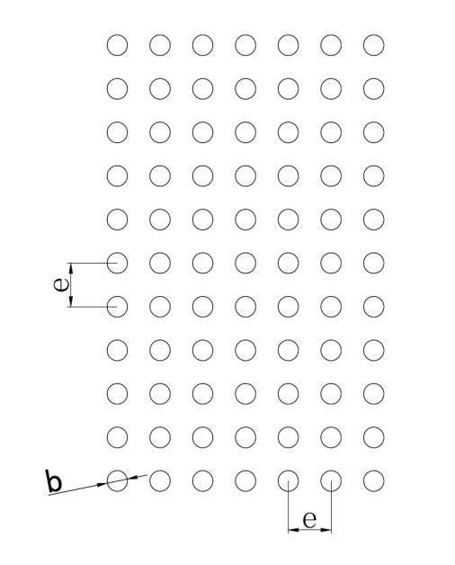
NSMD pad design. Pad dimension b = 0.63 mm; pitch e = 1.27 mm. Keep 3–5 mm clearance around the BGA; via-in-pad routing is prohibited in the source instructions.